A Sub-2 dB NF Dual-Band CMOS LNA for CDMA/WCDMA Applications
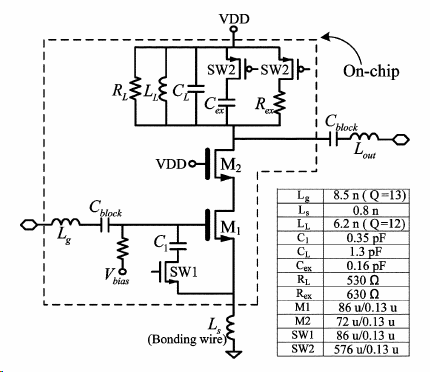
A dual-band LNA for the 1.8 GHz and 2.14 GHz operations with on chip switches is proposed. By switching the extra capacitor in parallel with the of the main transistor for input matching and the harmonic tuned load for output matching, the LNA achieves the minimal performance degradation by the switching operation. Using a 0.13- CMOS process, the designed compact dual-band LNA consumes 7.5 mW. All components are integrated on a single-chip except the blocking capacitor and series inductor. It exhibits a 14.54 dB/16.6 dB gains and a 1.75 dB/1.97 dB noise figures at the 1.8 and 2.14 GHz, respectively.
Fig. 1. Schematic of the dual-band LNA with switching components
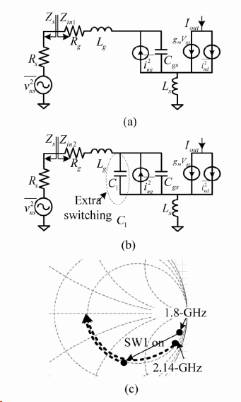
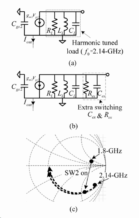
Fig. 2. Small Signal model of input/output circuit at each frequency bands and matching on Smith chart
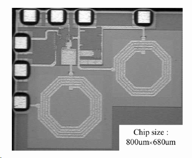
Fig. 3. Chip photograph of the proposed dual-band LNA
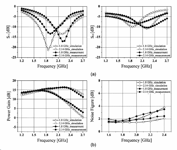
Fig. 4. Simulation and Measurement Results
[Ref.] Hyejeong Song, Huijung Kim, Kichon Han, Jinsung Choi, Changjoon Park, and Bumman Kim, "A sub-2 dB NF dual-band CMOS LNA for CDMA/WCDMA applications," IEEE Micorwave and Wireless Components Letters, vol. 18, no. 3, pp. 212-214, Mar. 2008.