![]() PAM Based on the Load Modulation
PAM Based on the Load Modulation
Introduction
Recent mobile handsets for CDMA systems require highly linear and efficient power amplifiers (PAs) in order to maximize the standby and talk times. The PAs must be designed and manufactured to meet the output power specification of the system with maximum output of 28dBm and ACPR under 48dBc, while maximizing the efficiency. The PAs deliver usually a high efficiency only at near the maximum rated power level, and the efficiency drops drastically as the output power level is reduced. Therefore, we can increase the talk-time by reducing the average current at the low power level the power amplifier operates mostly at a low efficiency region. Therefore, it is desirable to enhance the efficiency at the usual operation power level.
The load modulation scheme, which is described by the Doherty, is the most promising solution for the handset application, because it has simpler circuit topology than others such as Kahn (Envelope Elimination and Restoration), LINC (LInear amplification using Non linear Components), bias adaptation, and so on.
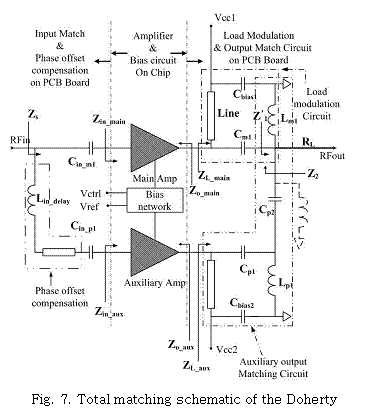
The classical Doherty amplifier uses a λ/4 transmission line for the load modulation, but it is not suitable for handset amplifier application due to the large size. To apply the load modulation technique to a handset power amplifier, the λ/4 transmission line is replaced by a lumped LC π-network. Based on the circuit, we have demonstrated a linear power amplifier with a high efficiency at the back-off region using GaAs HBT technology.
Principle of load modulation by the size ratio (N) of Main and auxiliary amplifiers
A. Load modulation technique.
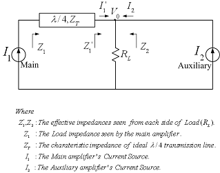
Figure 1. Operation diagram of load modulation

Figure 2. Z1’ and Z2 by the variation of α with RL= 50 Ω and ZT = 50 Ω
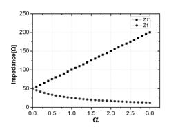
Figure 3. Z1’ and Z1 by the variation of α with RL= 50 Ω and ZT = 50 Ω
B. The efficiency of the Doherty amplifier

Fig 5. Efficiency of The Doherty amplifier by the size ratio [N]
Replacement of λ/4 transmission line with LC network
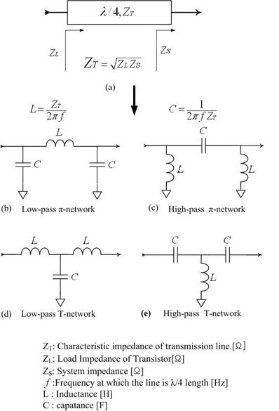
Fig. 6 The equivalent circuit topology of λ/4 transmission line using lumped elements.
Implementation & performance
A. Doherty amplifier for cellular handset amplifier.
N=1 N=3
Fig. 8. Photographs of Doherty amplifier by the size ratio [N].
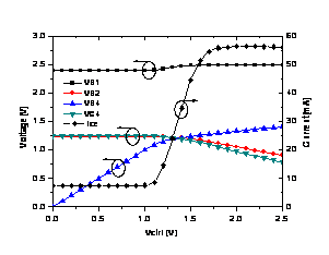
B. Performance of the Doherty amplifier by the size ratio [N]
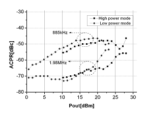
(a) Gain & Efficiency (b) ACPR at offsets of 885KHz and 1.98 MHz
Fig. 9 RF power and linearity performances of Doherty amplifier with size ration N=1
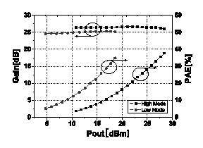
(a) Gain & Efficiency (b) ACPR at offsets of 885 KHz and 1.98 MHz
Fig. 10 RF power and linearity performances of Doherty amplifier with size ration N=3
Dynamic bias controlled Doherty amplifier.
A. bias control circuit.
(a) proposed dynamic bias control circuits
(b) simulated voltage and current curves of the bias control circuit according to the control voltage
Fig. 11 proposed base bias control circuit
B The Photographs of The Dynamic bias controlled Doherty amplifier
(a) The MMIC chip of Doherty PA. (b) The Modules for RF power test.
Fig. 12 the Photographs of Dynamic bias controlled Doherty Power Amplifier.
C. Performance of proposed dynamic bias controlled Doherty amplifier.
(a) ACPR at 885 KHz offset vs Pout for each bias condition (b) PAE Vs Pout for each bias condition
Fig. 13 RF performance of dynamic bias controlled Doherty PA.
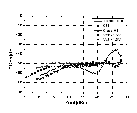
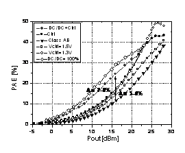
The comparison of the each power amplifiers’ average currents.
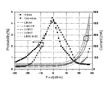
Fig. 14 PDF & DC currents vs Pout for each bias condition.


Reference
[1]. Joongjin Nam, Youngwoong Kim, Jin-Ho Shin, and Bumman Kim, “A CDMA and AMPS Handset Power Amplifier based on Load Modulation Technique," Proc. 34th European Microwave Conf. digest, Amsterdam, Netherlands, EuMC2004,pp329-332 and 12th GAAS2004, pp. 523- 526,Oct., 2004.
[2] Joongjin Nam, Jin-Ho Shin, and Bumman Kim “Load modulation power amplifier for IEEE 802.11b/g WLAN applications," IEE Electronics Letters, Vol.42, No. 1, pp. 24- 25, Jan., 2006.
[3] Joongjin Nam, Jin-Ho Shin, and Bumman Kim, “A Handset power amplifier with High Efficiency at a Low Level using Load Modulation Technique,” IEEE Trans. Microwave Theory Tech, Vol. 53, No. 8, pp. 2639 - 2644, Aug., 2005.
[4] Joongjin Nam, and Bumman Kim,”The Doherty Power amplifier with On-Chip Dynamic Bias Control Circuit for Handset Application” submitted to IEEE Trans, Microwave Theory Tech. Sept. 2006.
[5] Joongjin Nam, Jin-Ho Shin, and Bumman Kim, “The Handset Power Amplifier using Continuous Bias Control," 20th ITC-SCSS 2005 Jeju, Korea, Vol. 4, pp.1265-1266 July, 2005.
[6] Joongjin Nam, and Bumman Kim, “The Handset Power Amplifier with On-Chip Dynamic Bias Control Circuit to reduce Average Current” Submitted to IEEE Trans. Microwave Theory Tech. July. 2006.
[7][Invited] Bumman Kim, Joongjin Nam, Daekyu Yu. “Doherty Linear Power Amplifiers for Mobile Handset Applications”, will be published in APMC 2006 Dec. 2006.
[8][Invited] Bumman Kim, Joongjin Nam, Daekyu Yu. “Doherty Linear Power Amplifiers for Mobile Handset Applications”, will be published in RWS 2007 Jan. 2007.
![]() Fully Integrated Doherty Power Amplifiers
Fully Integrated Doherty Power Amplifiers
Abstract
Fully integrated Doherty amplifiers have been developed for 5 GHz wireless-LAN (WLAN) applications. Through a new Doherty power amplifier circuit topology, the bulky Doherty in/output matching block including quarter-wave (λ/4) impedance transformer can be fully integrated using capacitors, short micro-strip lines and bonding wires. To improve efficiency at a full power, without using the bulky input power splitter, a new input power driving concept is implemented by inserting λ/4 impedance transformers at the inputs of the carrier and peaking amplifiers using the lumped elements. The amplifier based on InGaP HBT technology, shows an output power of 22.5 dBm and a power-added efficiency (PAE) of 21.3 % at an error vector magnitude (EVM) of 5 %, measured with 54 Mbps 64-QAM-OFDM signals at 5.2 GHz. The proposed in/output matching topology allows the fully integrated Doherty amplifiers with a small size.
Design Description For A Fully Integrated-Doherty PA
A. Doherty Circuit Topology Description for Miniaturization
In a π-type equivalent lumped circuit of the transformer, the inductance is in proportion to characteristic impedance (Zo). Therefore, it is preferred to match the output load impedance from 50 Ω to a suitably low value Ropt/2 for a low Zo. In case of the Ropt of 5.8 Ω and center-frequency (fo) of 5.2 GHz, the inductance in π-type equivalent lumped circuit is reduced to 0.17 nH and can be replaced by a micro-strip line with 200~300 μm length on MMIC chip. To prevent the power leakage into off-state peaking amplifier in low power ranges, the output impedance of the peaking amplifier should be transformed to nearly open using another offset line. Because the characteristic impedance of offset line is the optimum load impedance (Ropt), the offset line can be easily integrated on MMIC chip, too.
Additionally, a simple and small sized second harmonic termination circuit is realized with integrated MIM capacitors and bonding wires at the end of the carrier and peaking amplifier collectors. The bonding wires for the resonance at 2fo can be tuned by adjusting the length of the wires.
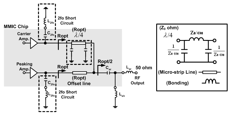
Fig. 1. Schematic diagram of the new Doherty output matching circuit for miniaturization
A schematic diagram of the new Doherty output matching circuit with miniaturization of the transformer is shown in Fig. 1. The output matching circuit consists of MIM capacitors (Csr and C2fo) on the MMIC chip and bonding wires (Lsh, Lsr, and L2fo) connecting MMIC chip with a PCB module substrate. The bonding wires are used as inductors, whose size, cost and loss are far better than those of on-chip spiral inductors and micro-strip transmission lines on PCB substrates. Thus, the chip size can be small and efficiency is high.
B. New Uneven Power Drive in Doherty PA
Because the peaking power cell has been biased lower than the carrier one, the current level of the peaking cell at the maximum input drive can not reach the maximum allowable current level. Thus, the load impedances of both cells can not be fully modulated to the optimized impedances. As a result, the conventional Doherty power amplifier has been heavily saturated, and it degrades linearity and produces far less power. In our earlier work, we propose the uneven power driving for base station power amplifiers application , applying more power to the peaking power cell. In the drive, the peaking cell is opened fully and the load impedances are modulated completely. The concept can be applied for Doherty amplifier for the mobile application with suitable modification for the small chip design. Because of applying less power to carrier power cell, it leads to not only power gain loss but also reduce efficiency at low and medium power levels. So we propose a new uneven power driving concept in Fig. 2 (b). At a low or medium power level, the more power is applied to the carrier power cell for the increase a power gain and efficiency. On the other hand, the more power is applied to the peaking power cell at a high power to reach the maximum allowable current level of the cell.
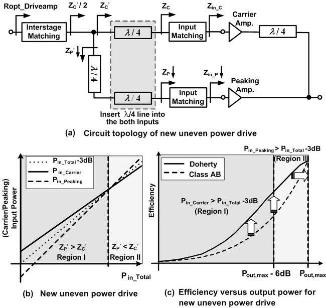
Fig. 2. New uneven power drive concept in the handset Doherty power amplifiers.
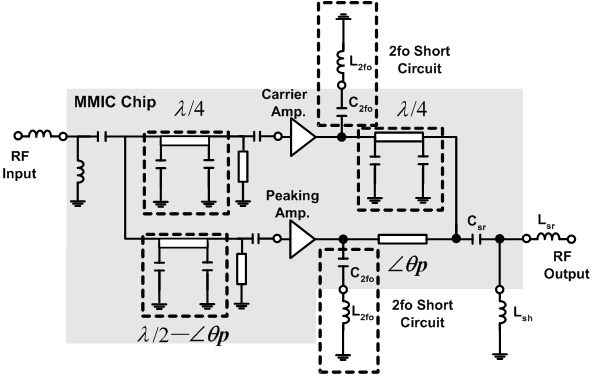
Fig. 3. Simplified schematic circuit diagram of Doherty power amplifiers for the 5 GHz WLANs.
The new uneven power drive can be achieved without using bulky 3 dB hybrid coupler or power divider. The input impedance of the carrier power cell (Zin_C) does not change considerably according to the input power level. On the other hand, the input impedance of the peaking power cell (Zin_P) decreases considerably as the input power increases due to the self biasing effect. We can utilize the effect. In conventional Doherty topology, due to the λ/4 delay line in front of the peaking amplifier, the impedance of the peaking amplifier increases as the power level increases. Therefore, a less power is delivered to the peaking amplifier. To solve the problem, we insert λ/4 impedance transformers at the in ports of the carrier and peaking amplifiers as shown in Fig. 2 (a). As the input power level becomes higher, more input power is applied to the peaking power cell and less to the carrier. A simplified schematic circuit diagram of the Doherty power amplifier with new uneven power driving is shown in Fig. 3.
Fabrication and Experimental Results
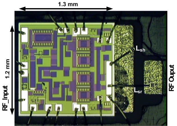
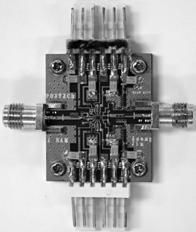
Fig. 4. Photograph of fully integrated Doherty power amplifiers with bonding wires.
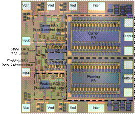
The commercial 2μm InGaP/GaAs HBT foundry is employed to fabricate the MMIC chip. The emitter size of each InGaP/GaAs HBT is 2 μm x 20 μm x 2 fingers (unit cell). To obtain an output power of more than 28 dBm, 32 unit cells are employed for the output stages of carrier and peaking power amplifiers, respectively. Fig. 4 shows a photograph of the fully integrated Doherty power amplifier module consisting of an HBT MMIC with 3-stage HBT power amplifier and bonding wires. The MMIC chip area is 1.2 mm x 1.3 mm.
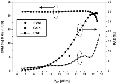
Fig. 5. Measured power characteristics of the fabricated Doherty power amplifiers with 54 Mbps 64-QAM-OFDM signals at 5.2 GHz.
Fig. 5 shows the power measurement results of the fabricated amplifier with 54 Mbps 64-QAM-OFDM signal at 5.2 GHz and supply voltage VCC of 3.3 V. The quiescent currents of the 1st, 2nd derive amplifiers, and carrier amplifier are 10, 36, and 50 mA, respectively. From the figure, P1dB and power gain of the fabricated power amplifier is 28.4 dBm and 21.5 dB, respectively. The PAE at P1dB is 29.5 %. At an EVM of 5 %, PAE of 21.3 % and an output power Pout of 22.5 dBm are achieved. We estimate the performance at Class AB operation by adjusting the peaking amplifier bias equal tothe carrier amplifier one. The PAE at an output power Pout of 22.5 dBm is 16.6 %, which is an 4.7 % improvement. In the amplifier, RF power gain of the power stage in Doherty action, is very low, about 6 dB. As the RF power gain of power stage is increased, the PAE of Doherty power amplifier can be improved further.
Reference
1. Daekyu Yu, Yong-woong Kim, Kichon Han, Jin-ho Shin, and Bumman Kim, “ Fully Integrated Doherty Power Amplifiers for 5 GHz Wireless-LANs,” IEEE Radio Frequency Integrated Circuits (RFIC) Symp., San Francisco, CA(USA), pp. 177-180, June, 2006.