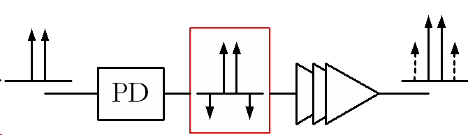
1. Introduction to Predistortion Techniques
In current,wireless communication systems such as IS-95 series, CDMA(code division multiple access)-2000, WCDMA( wide-band code division multiple access ), etc., highly linear power amplifiers are in great demand.To meet the stringent requirement for linearity, various linearization techniques are adopted. Among the techniques, the feed-forward method provides extremely linear and broad-band characteristics. However, it is an expensive solution, consisting of auxiliary error amplifiers and complicated control circuits. On the other hand, a feedback technique has decisive disadvantages of instability and bandwidth limitation. Hence, a predistortion technique is preferred for linear power amplifiers due to simple structure and low cost.
2. Analog Predistortion Techniques
![]() Predistortion
RF Power Amplifier for Multicarrier WCDMA applications
Predistortion
RF Power Amplifier for Multicarrier WCDMA applications
We analyzed the effects of linearity degradation factors of a predistorter such as a higher order term, amplitude, and phase mismatches. Based on the data, we find the level to which a predistortion power amplifier can be maximally linearized with CDMA signals. For this purpose, a simple and general third-order predistorter is used. Instead of just adjusting the predistorter for the amplifier, we optimize the amplifier and predistorter as a pair. In order to verify our analyses, a predistortion power amplifier is implemented and tested using a IS-95 CDMA signal and a four-carrier WCDMA signal. The test results show superior performances.
A. Implementation of a Third-Order Predistorter
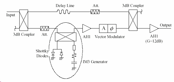
Fig. 1. Circuit diagram of the third-order predistorter
The power amplifier was designed using Motorola’s MRF21030 LDMOSFET with a 30-W peak envelope power (PEP) and an MHL21336 driver.
(a)
(b) (c)
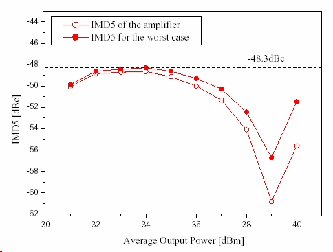
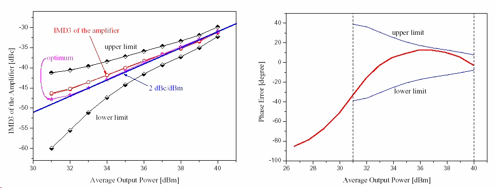
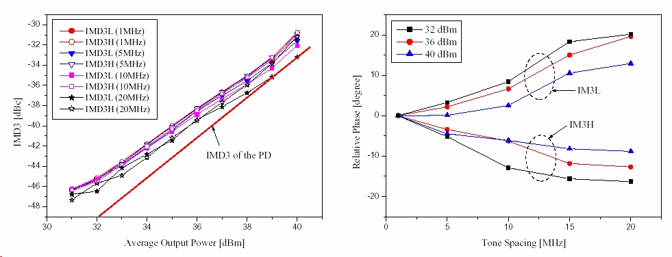
Fig. 2. Two-tone IM characteristics of the amplifier according to the power levels. (a) IMD5. (b) IMD3. (c) Phase error of IM3.
B. Reduction of Memory Effect
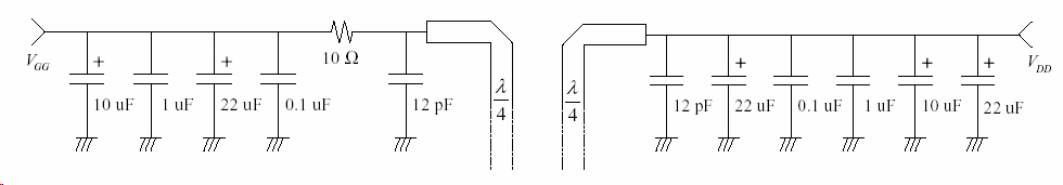
Fig. 3. Bias circuits for reduction of memory effects: Gate and drain bias circuits.
(a) (b)
Fig. 4. Measured IM3 characteristics of the amplifier according to tone spacings. (a) IMD3. (b) Phases.
C. Linearization for WCDMA 4FA signal
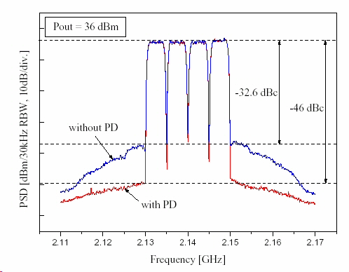
Fig. 5. Linearized spectrum for a four-carrier WCDMA signal at 36 dBm.
For a linear RF power amplifier with a third-order predistorter, we have analyzed the three basic performance degradation factors using a two-tone signal. The factors include the IMD5 level of the amplifier, and the amplitude and phase errors for the IM3 terms. The IMD5 level limits linearization performance. We have quantitatively derived the allowable amplitude error without any phase error, the permissible phase-error range with a given amplitude error, and the optimum amplitude error for a given phase error.
In order to hold a good cancellation performance for a fourcarrier WCDMA signal with a 20-MHz signal band, we have tried to reduce the memory effects of the amplifier. A proper design of the gate- and drain-bias circuits gives an amplitude error less than 2 dB and an average phaseerror difference less than 21 between lower and upper IM3s over the considered total power range. These additional errors caused by memory effects have slightly degraded the linearization performance for a four-carrier WCDMA signal. The predistortion power amplifier has displayed an ACLR of 46 dBc with 13.4-dB cancellation at 5-MHz offset. We expect that our analysis will assist for a design of the predistortion power amplifier.
![]() Analog
Predistortion Linearizer for High-Power RF Amplifiers
Analog
Predistortion Linearizer for High-Power RF Amplifiers
Analog predistortion linearizers are smaall, inexpensive and consume low power, but only moderate linearity improvement can be achieved with this technique. We have developed analog predistorter that can control the magnitude and phase of third and fifth intermodulation distortion components independently.
We have employed a power amplifier with an average output power of 45 dBm and a peak power of 450 W. The amplifier consists of two parts: the driver and main amplifier. The driver is an LDMOS-based three-stage amplifier, and a 30-W LDMOS is used at the final stage to drive the main amplifier. The main amplifier is two stages. One stage is a 120-W LDMOS and the final stage is a four-way combined 120-W LDMOS, which can handle 450 W of peak power in a CDMA signal. The amplifier operates in class AB and the overall gain of the main amplifier is about 50 dB.
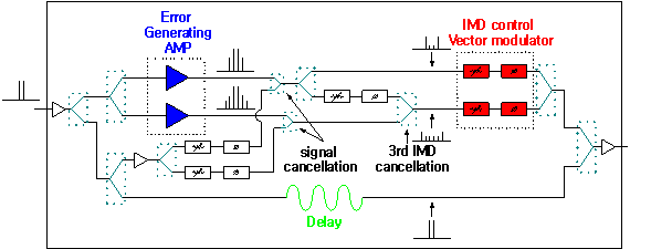
Fig. 1. Circuit diagram of modified predistortion circuit configurations.
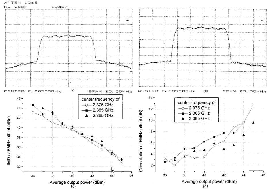
Fig. 2. Spectral regrowth. (a) Before linearization. (b) After linearization. (c) Spectral regrowth of the main amplifier. (d) Suppression of spectral regrowth for different power levels. (a) Before linearization (at average output power of 45 dBm). (b) After linearization (at average output power of 45 dBm). (c) Spectral regrowth versus output power for the main amplifier at 5-MHz offset from several center frequencies (measured IMD is the difference of the spectral power at the center and offset frequencies). (d) Suppression of spectral regrowth for different power levels.
We have developed a predistortion linearizer that can control the IM3 and IM5 separately and applied it to the linearization of a high-power RF amplifier with an average output level of 45 dBm. The phase variations of the IM terms are accurately measured using the new method and the data is employed for the predistorter design. About 9-dB improvement of adjacent channel leakage ratio (ACLR) was achieved at 5-MHz offset from the center frequency of a CDMA signal with an 8.192-MHz signal bandwidth. This amplifier covers a 2.37–2.4-GHz bandwidth.
![]() New Predistortion Linearizer Using Low-Frequency Even-Order Intermodulation
Components
New Predistortion Linearizer Using Low-Frequency Even-Order Intermodulation
Components
We present two types of new predistortion linearizers using low-frequency even-order components. One adopts an in-phase and quardrature balanced modulator as a generator of the third-order intermodulation (IM3) and fifth-order intermodulation (IM5) components and the other adopts a double-balanced diode mixer. Both types are very compact and could independently control the amplitudes and phases of the intermodulation (IM) components.
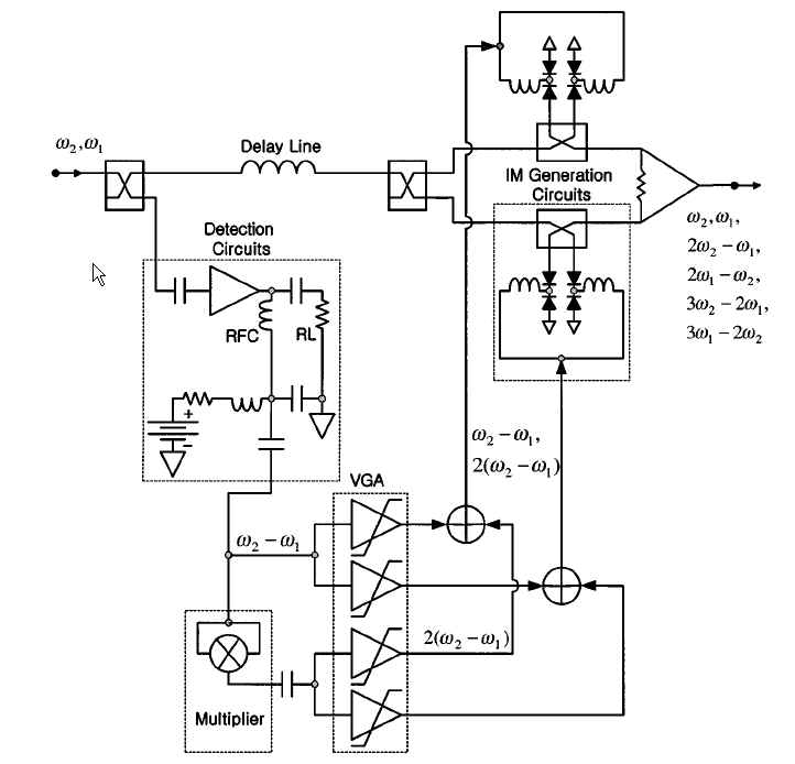
Fig. 1. Block diagram of the new predistortion linearizer using an I/Q balanced modulator as an IM generation circuit.
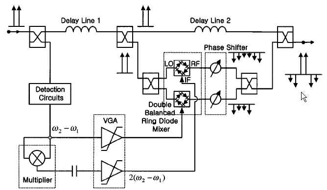
Fig. 3. Block diagram of the new predistortion linearizer using a double-balanced diode mixer as an IM generator.
To validate the proposed predistortion linearizers, two types of the predistorters are implemented. In both cases, we have used the same detection circuits. They consist of Mini-circuit’s ERA-5SM as a low-frequency second-order IM generator, a 50- load resistor as an RF termination, an RF choke inductor, a series inductor, a resistor to choke a detected signal, and a large capacitor to bypass the detected signal. The main amplifier is composed of a single driver stage and a final power stage (Motorola’s MHL21336, 35-dBm amplifier) with a total gain of 30.7 dB. The analog circuits including a multiplier, voltage-controlled VGA, and adder are designed to have at least 25-MHz bandwidth for broad-band linearization. TheVGA was designed to have a positive or a negative gain polarity according to the control voltage. The analog circuits’ delay is compensated by a coaxial delay line, which is about 18 ns in this experiment.
The IM generation circuit of the first type consists of varactor diodes connected to a reflection-type 90 hybrid coupler. The dc bias is properly assigned to the varactor diodes to prevent generation of any higher order components since only the second-order coefficient of the phase modulation characteristics of the varactor diode is used.
In the predistortion linearizer using a double-balanced diode mixer, an RF phase shifter is built using varactor diodes in reflection type to have more than a 180 tuning dynamic range. The double-balanced mixer is RF prime’s RFMT-25H. Delay line 1 compensates for the low-frequency circuit delay and delay line 2 compensates for the delay of the mixer and phase shifter.
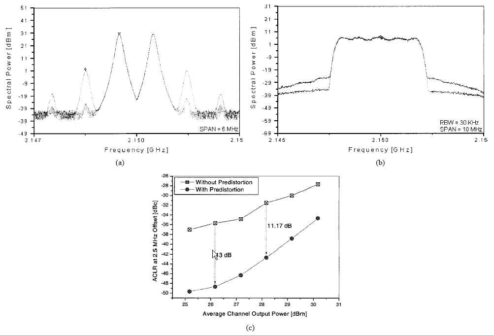
Fig. 3. Linearization results of the predistorter using an I/Q balanced modulator. (a) For a two-tone test spectra. (b) For a broad-band CDMA spectra with a chip rate of 4.096 Mc/s and an average output channel power of 28.17 dBm. (c) For ACLR versus average output channel power of a broad-band CDMA signal at 2.5-MHz offset frequency.
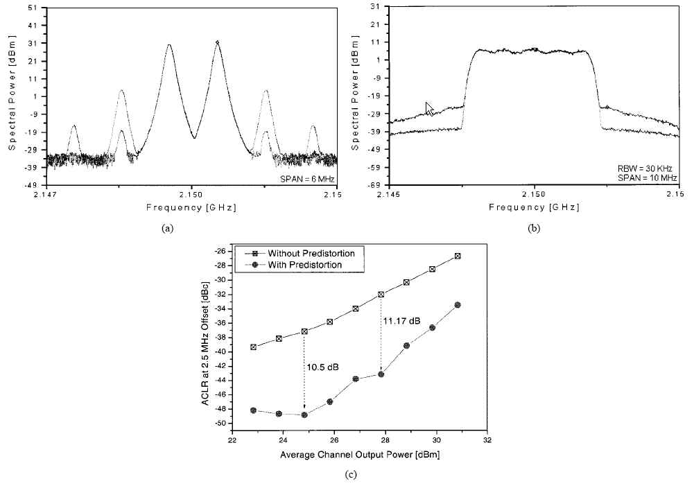
Fig. 4. Linearization results of the predistorter using a double-balanced mixer. (a) For a two-tone test spectra. (b) For a broad-band CDMA spectra with a chip rate of 4.096 Mc/s and an average output channel power of 28.83 dBm. (c) For ACLR versus average output channel power of a broad-band CDMA signal at 2.5-MHz offset frequency.
To validate the proposed predistortion linearizers, a two-tone linearization test and a broad-band CDMA linearization test are performed at the IMT-2000 band of 2.15 GHz. The results show that significant cancellations are achieved for both the IM3 and IM5 components. The broad-band CDMA test and its power sweeping test showthat the ACLR is improved by over 11.17 dB at an optimized average channel output power and the improvement is maintained through a broad range of the power levels.
These predistorters can be easily linked into appropriate adaptation control circuits because both circuits use only four control parameters and the compact sizes of the predistorters are convenient for adding spaces for adaptive control circuits.
Reference
[1] J. Yi, Y. Yang, M. Park, W. Kang and B. Kim, "Analog predistortion Linearizer for high power RF amplifier," IEEE Trans. Microwave Theory and Technique, Vol.48, No.12,pp. 2709-2713, Dec. 2000
[2] Y. Yang, Y. Y. Woo, B. Kim, "New Predistortion Linearizer using Low Frequency Even Order Intermodulation Components." IEEE Trans. Microwave Theory Tech. Vol 50, No.2, pp446-452, Feb., 2002
[3] J. Cha, J. Yi, J. Kim, and B. Kim "Optimum Design of a Predistortion RF Power Amplifier for Multi-Carrier WCDMA Applications" IEEE Trans. Microwave Theory Tech., Vol. 52, No.2, Feb. 2004. pp.655 - 663